
onsemi and Innoscience Announce Plans to Collaborate to Speed Global Rollout of GaN Power Portfolio
Collaboration would add high-volume, cost-optimized, worldwide GaN manufacturing for faster market deployment of energy-efficient power devices
Summary:
onsemi announced it has signed a memorandum of understanding with Innoscience to explore expanding production of gallium nitride (GaN) power devices using Innoscience’s proven 200mm GaN-on-silicon process. The collaboration would combine onsemi’s system integration, drivers, and packaging expertise with Innoscience’s GaN wafers and high-volume manufacturing leadership in an effort to bring cost-effective, energy-efficient solutions to market faster and accelerate GaN adoption.
News Highlights:
- Collaboration would expand onsemi’s low and medium-voltage GaN power portfolio and scale GaN manufacturing worldwide for faster market availability and greater adoption.
- The non-binding MOU outlines a strategic partnership, including wafer procurement and extended collaboration, leveraging onsemi's GaN power solutions and Innoscience's leading wafer manufacturing to target the projected $2.9 billion total addressable market1 by 2030 for GaN power devices, with the potential value in the hundreds of million dollars for both companies.
- The arrangement would assist onsemi and Innoscience in their efforts to deliver significant customer value, specifically by combining onsemi’s expertise in packaging, drivers, and systems integration with Innoscience’s proven wafer manufacturing capabilities.
- The two companies’ technologies together are expected to enable smaller, more efficient GaN solutions for industrial, automotive, telecom infrastructure, consumer, and AI data center markets.
SCOTTSDALE, Ariz., and SUZHOU, China, Dec. 02, 2025 (GLOBE NEWSWIRE) -- onsemi and Innoscience today announced the signing of a memorandum of understanding (MoU) to evaluate opportunities to accelerate deployment of GaN power devices, starting with 40-200V, and significantly broaden customer adoption. The collaboration outlined in the MoU brings together onsemi’s leadership in integrated systems and packaging with Innoscience’s proven GaN technology and high-volume manufacturing to enable delivery of cost-effective, highly efficient GaN products for industrial, automotive, telecom infrastructure, consumer and AI data center markets.
GaN semiconductor devices offer higher switching speeds, smaller form factors, and lower energy losses to deliver more power in less space. Until now, limited offerings and manufacturing capacity have slowed GaN adoption in the low and medium-voltage segment. Through this collaboration, onsemi and Innoscience will seek to overcome these barriers to quickly bring high-volume, worldwide deployment of optimized GaN solutions for mainstream markets:
- Industrial: motor drives for robotics, solar microinverters, and optimizers
- Automotive: DC-DC converters, synchronous rectification
- Telecom Infrastructure: DC-DC and point-of-load converters
- Consumer and Mass Market: power supplies, adaptors, DC-DC converters, motor drives, audio, light e-mobility, power tools, robotics
- AI Data Center: intermediate bus converters, DC-DC converters, battery backup units
For onsemi customers, the collaboration with Innoscience would enable:
- Faster Time to Market: Rapid prototyping, accelerated design-in, and swift entry into mainstream markets with onsemi's system expertise and Innoscience’s proven GaN technology and manufacturing
- Scalable Manufacturing: True mass-market scalability to handle large-volume ramps, leveraging onsemi's global integration and packaging experience and Innoscience’s established GaN capacity
- Lower System Cost: Optimized package, fewer components and simplified thermal management deliver more compact designs and lower total system cost
“As power demands rise across every sector, GaN offers higher efficiency, smaller size, and lower energy losses compared to other materials. Until now, in the low and medium voltage segments, cost and supply constraints have limited its widespread adoption. Through a collaboration with Innoscience, we expect to be able to access the industry’s largest GaN production footprint and quickly scale our GaN offerings for customers worldwide to enable broader adoption in mainstream power applications." – Antoine Jalabert, Vice President of Corporate Strategy, onsemi
“GaN technology is essential to improving electronics, creating smaller, more efficient power systems, saving electric power, and reducing CO2 emissions. Innoscience is excited to explore a strategic collaboration opportunity with onsemi, to expand and accelerate the adoption of GaN power worldwide, and to create a system integration platform with onsemi’s broad portfolio.” – Yi Sun, Senior Vice President, Product & Engineering
A Complete Intelligent Power Portfolio
GaN is projected to capture an estimated $2.9 billion, or 11% share, of the global power semiconductor market by 2030, with a projected compound annual growth rate from 2024-2030 of 42%1. This collaboration with Innoscience would build on onsemi’s comprehensive intelligent power portfolio, which now spans silicon, silicon carbide (SiC), and GaN technologies. Together, these technologies enable onsemi to deliver the optimal power system for application across AI data center, automotive, industrial, and consumer. This complete low and medium voltage portfolio strengthens onsemi’s position as a leading provider of fully integrated power systems to help customers maximize performance and energy efficiency as global electrification and AI-energy demand continues to surge.
Timing and Availability
onsemi expects to begin sampling in the first half of 2026.
1 Source: Yole Power GaN 2025
Caution Regarding Forward-Looking Statements:
This press release includes “forward-looking statements,” as that term is defined in Section 27A of the U.S. Securities Act of 1933, as amended, and Section 21E of the U.S. Securities Exchange Act of 1934, as amended. All statements, other than statements of historical facts, included or incorporated in this press release could be deemed forward-looking statements, particularly statements about the state and potential impacts of any collaboration between onsemi and Innoscience. Forward-looking statements are often characterized by the use of words such as “believes,” “estimates,” “expects,” “projects,” “may,” “will,” “intends,” “plans,” “anticipates,” “targets,” “should,” “would” or similar expressions or by discussions of strategy, plans, expectations, projections or intentions. All forward-looking statements in this document are made based on onsemi’s current expectations, forecasts, estimates and assumptions and involve risks, uncertainties and other factors that could cause results or events to differ materially from those expressed in the forward-looking statements. Certain factors that could affect onsemi’s future results or events are described under Part I, Item 1A “Risk Factors” in the 2024 Annual Report on Form 10-K that onsemi filed with the U.S. Securities Exchange Commission (“SEC”) on February 10, 2025 (the “2024 Form 10-K”) and from time to time onsemi’s other SEC reports. Readers are cautioned not to place undue reliance on forward-looking statements. onsemi assumes no obligation to update such information, which speaks only as of the date made, except as may be required by law. Investing in onsemi’s securities involves a high degree of risk and uncertainty, and you should carefully consider the trends, risks and uncertainties described in this document, the 2024 Form 10-K and other reports filed with or furnished to the SEC by onsemi before making any investment decision with respect to onsemi’s securities. If any of these trends, risks or uncertainties actually occurs or continues, onsemi’s business, financial condition or operating results could be materially adversely affected, the trading prices of onsemi’s securities could decline, and you could lose all or part of your investment. All forward-looking statements attributable to onsemi or persons acting on onsemi’s behalf are expressly qualified in their entirety by this cautionary statement.
About onsemi
onsemi (Nasdaq: ON) is driving disruptive innovations to help build a better future. With a focus on automotive and industrial end-markets, the company is accelerating change in megatrends such as vehicle electrification and safety, sustainable energy grids, industrial automation, and 5G and cloud infrastructure. onsemi offers a highly differentiated and innovative product portfolio, delivering intelligent power and sensing technologies that solve the world’s most complex challenges and leads the way to creating a safer, cleaner and smarter world. onsemi is included in the Nasdaq-100 Index® and S&P 500® index. Learn more about onsemi at www.onsemi.com.
onsemi and the onsemi logo are trademarks of Semiconductor Components Industries, LLC. All other brand and product names appearing in this document are registered trademarks or trademarks of their respective holders. Although the Company references its website in this news release, information on the website is not to be incorporated herein.
About Innoscience
Innoscience (HKEX:02577.HK) is the global leader in 8” GaN-on-Silicon process innovation and power device manufacturing. Innoscience’s device designs and performance have set the worldwide standard for GaN, and Innoscience’s GaN products have achieved majority market share in multiple low, medium and high voltage applications, with GaN process nodes covering 15V to 1200V. Innoscience’s products are well-known for reliability, performance, and functionality in consumer, automotive, data center, and renewable energy sectors. For more information, please visit http://www.innoscience.com/.
Contact:
onsemi
Michael Mullaney
michael.mullaney@onsemi.com
+1 838-289-7314

- 海能达携手西安咸阳机场、重庆磁器口获评2025数字城市创新成果与实践案例
- 清能股份的多层增强AEM膜实现“高性能、长寿命”
- Fujirebio的Lumipulse® G pTau 217/ β-淀粉样蛋白1-42血浆比值体外诊断检测获得上市许可,辅助识别阿尔茨海默病相关淀粉样蛋白病变患者
- 发展稳健向上,初心坚定不移,阳光保险中报答卷新鲜出炉
- 央视点赞千寻位置:时空智能支持250万辆汽车实现高级辅助驾驶
- 5月19日纳木措开湖日即将启幕,系列文旅活动等你来
- 苏州雄海包装:包装领域的璀璨之星
- 寒冬送暖!桂林嘉城商贸 "春节门窗守护计划":免费维保暖特殊群体,诚信服务赢人心
- 国泰集团携手中国宋庆龄基金会设立“国泰航梦青少年发展基金”
- 徐成峰《智者无敌》刻画反派人物 戏路不受限制
- 沪上创新生命教育新模式——福寿园推出“生死教育家长绘本营”系列活动
- 容祖儿成为香港启德开幕首位表演歌手 高燃开场《越唱越强》见证荣耀时刻
- 国央实业开辟无人机国际物流运输新赛道,助力2025年海南自贸港封关运作
- 演员王子辰首次实力出演话剧引关注
- 2024 剑桥艺术上海校区CSVPA China升学喜报 艺术类全美前10本科直录大满贯
- 315行动 | “熊大爷”门店自查:守护舌尖安全,升级消费体验
- 第三届全国工业经济应用创新职业技能竞赛江苏省预赛成功举办
- Philip Morris International Releases Integrated Report Detailing Progress Towards Its Smoke-Free Vis
- 解码“成都金融”之五:成都推动金融开放助力高水平共建“一带一路”
- 明理文化津沽行暨中华石园迎新春首届非遗文化节盛大开幕
推荐
-
 看新东方创始人俞敏洪如何回应董宇辉新号分流的?
(来源:中国证券报)
东方甄选净利润大幅下滑
资讯
看新东方创始人俞敏洪如何回应董宇辉新号分流的?
(来源:中国证券报)
东方甄选净利润大幅下滑
资讯
-
 男子“机闹”后航班取消,同机旅客准备集体起诉
1月4日,一男子大闹飞机致航班取消的新闻登上
资讯
男子“机闹”后航班取消,同机旅客准备集体起诉
1月4日,一男子大闹飞机致航班取消的新闻登上
资讯
-
 一个“江浙沪人家的孩子已经不卷学习了”的新闻引发议论纷纷
星标★
来源:桌子的生活观(ID:zzdshg)
没
资讯
一个“江浙沪人家的孩子已经不卷学习了”的新闻引发议论纷纷
星标★
来源:桌子的生活观(ID:zzdshg)
没
资讯
-
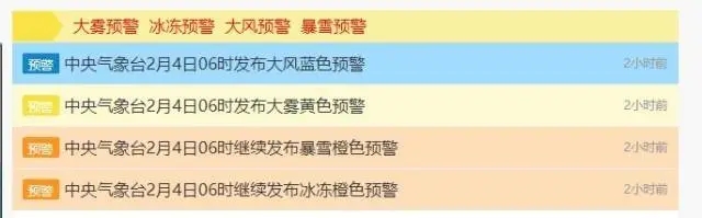 中央气象台连发四则气象灾害预警
暴雪橙色预警+冰冻橙色预警+大雾黄色预警+
资讯
中央气象台连发四则气象灾害预警
暴雪橙色预警+冰冻橙色预警+大雾黄色预警+
资讯
-
 大家一起关注新疆乌什7.1级地震救援见闻
看到热气腾腾的抓饭马上就要出锅、村里大家
资讯
大家一起关注新疆乌什7.1级地震救援见闻
看到热气腾腾的抓饭马上就要出锅、村里大家
资讯
-
 透过数据看城乡居民医保“含金量” 缴费标准是否合理?
记者从国家医保局了解到,近期,全国大部分地区
资讯
透过数据看城乡居民医保“含金量” 缴费标准是否合理?
记者从国家医保局了解到,近期,全国大部分地区
资讯
-
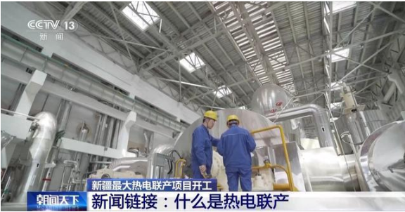 新增供热能力3200万平方米 新疆最大热电联产项目开工
昨天(26日),新疆最大的热电联产项目—&md
资讯
新增供热能力3200万平方米 新疆最大热电联产项目开工
昨天(26日),新疆最大的热电联产项目—&md
资讯
-
 周星驰新片《少林女足》在台湾省举办海选,吸引了不少素人和足球爱好者前来参加
周星驰新片《少林女足》在台湾省举办海选,吸
资讯
周星驰新片《少林女足》在台湾省举办海选,吸引了不少素人和足球爱好者前来参加
周星驰新片《少林女足》在台湾省举办海选,吸
资讯
-
 奥运冠军刘翔更新社交账号晒出近照 时隔473天更新动态!
2月20日凌晨2点,奥运冠军刘翔更新社交账号晒
资讯
奥运冠军刘翔更新社交账号晒出近照 时隔473天更新动态!
2月20日凌晨2点,奥运冠军刘翔更新社交账号晒
资讯
-
 王自如被强制执行3383万
据中国执行信息公开网消息,近期,王自如新增一
资讯
王自如被强制执行3383万
据中国执行信息公开网消息,近期,王自如新增一
资讯