
New ZEISS Crossbeam 750 FIB-SEM for high-accuracy sample preparation workflows
Advances in simultaneous SEM imaging while FIB milling provide unmatched feedback for precision endpointing
- New ZEISS Gemini 4 electron optics offer superior resolution and signal-to-noise ratio
- Live SEM imaging extended to monitor rapid FIB milling down to ultrafine lamella polishing
- Largest undistorted field-of-view supports the best outcomes in 3D tomography and APT workflows
ZEISS today unveiled the new ZEISS Crossbeam 750 focused ion beam-scanning electron microscope (FIB-SEM) that is optimized for demanding sample preparation. It provides a live, high-resolution “see while you mill” view at any imaging and milling condition to enable immediate feedback and eliminate milling interruptions for uniform first-pass transmission electron microscopy (TEM) lamellae and precise FIB cross sections.
For advanced semiconductor and materials workflows, ZEISS Crossbeam 750 FIB-SEM with new Gemini 4 electron optics delivers background-free, real-time endpointing and sub-nanometer precision for TEM lamellae and high-fidelity three-dimensional (3D) analysis. It is ideal for analysis of leading-node logic and memory devices as well as nanofabrication and 3D volume imaging. For materials research and life sciences, ZEISS Crossbeam 750 speeds acquisition times for 3D tomography through a larger field of view with reduced distortion.
“ZEISS Crossbeam 750 was designed around one core principle: Our customers should not have to stop milling to see where in their sample they are working,” said Dr. Thomas Rodgers, Senior Director of Market Strategy, Head of Business Sector Electronics, ZEISS Microscopy. “Our new high-dynamic-range (HDR) Mill + SEM capability maintains a clear, high-resolution SEM view at any FIB condition, from rapid milling with high FIB currents down to fine polishing at 0.5 kV. This real-time clarity, paired with Gemini 4 electron optics, allows customers to fine-tune processes as they work—reducing rework, improving yield and delivering highly uniform lamellae on the first pass.”
“See while you mill” transforms advanced semiconductor analysis
As semiconductor device architectures shrink and complexity increases—from fin field-effect transistor (finFET) to gate-all-around (GAA), complementary field-effect transistor (CFET), and emerging two-dimensional (2D) materials—precise, real-time control during FIB processing has become critical. ZEISS Crossbeam 750 directly addresses this need by maintaining a clear, high-resolution SEM view during milling, even at low landing energies and at tilt.
The system enables users to observe FIB-sample interactions in real time, fine-tune thinning and polishing steps as they occur, and to hit nanometer-scale endpoints on the first attempt—achieving consistent lamella quality for leading-node logic and memory device and backside power delivery network workflows.
Imaging excellence drives scientific discovery
ZEISS Crossbeam 750 FIB-SEM is essential in materials science workflows for uniform TEM lamella preparation, atom probe tomography (APT) sample prep, nanofabrication (including electron-beam lithography), and high-fidelity 3D volume imaging. For life sciences and materials research, the undistorted large field-of-view of ZEISS Crossbeam 750 and stable low-kV performance improves signal-to-noise and speeds acquisition time.
The ZEISS Crossbeam 750 FIB-SEM is available for ordering now. For more information, please click here.
Press contact
ZEISS Research Microscopy Solutions
Kristin Unger
Email: press.microscopy@zeiss.com
About ZEISS
ZEISS is an internationally leading technology enterprise operating in the fields of optics and optoelectronics. In the previous fiscal year, the ZEISS Group generated annual revenue totaling almost 12 billion euros in its four segments Semiconductor Manufacturing Technology, Industrial Quality & Research, Medical Technology, and Consumer Markets (September 30, 2025).
For its customers, ZEISS develops, produces, and distributes highly innovative solutions for industrial metrology and quality assurance, microscopy solutions for the life sciences and materials research, and medical technology solutions for diagnostics and treatment in ophthalmology and microsurgery. The name ZEISS is also synonymous with the world's leading lithography optics, which are used by the chip industry to manufacture semiconductor components. There is global demand for trendsetting ZEISS brand products such as eyeglass lenses, camera lenses, and binoculars.
With a portfolio aligned with future growth areas like digitalization, healthcare, and Smart Production and a strong brand, ZEISS is shaping the future of technology and constantly advancing the world of optics and related fields with its solutions. The company's significant, sustainable investments in research and development lay the foundation for the success and continued expansion of ZEISS' technology and market leadership. ZEISS invests 15 percent of its revenue in research and development – this high level of expenditure has a long tradition at ZEISS and is also an investment in the future.
With over 46,600 employees, ZEISS is active globally in around 50 countries with more than 60 sales and service locations, around 40 research and development facilities, and 30 production facilities worldwide (September 30, 2025). Founded in 1846 in Jena, the company is headquartered in Oberkochen, Germany. The Carl Zeiss Foundation, one of the largest foundations in Germany committed to the promotion of science, is the sole owner of the holding company, Carl Zeiss AG.
Further information at www.zeiss.com
ZEISS Research Microscopy Solutions
ZEISS Research Microscopy Solutions is the leading provider of light, electron, X-ray microscope systems, correlative microscopy and software solutions leveraging AI technologies. The portfolio comprises of products and services for life sciences, materials and industrial research, as well as education and clinical routine applications. The unit is headquartered in Jena. Additional production and development sites are located in Germany, UK, USA, China and Switzerland. ZEISS Research Microscopy Solutions is part of the Industrial Quality & Research segment.
Further information at www.zeiss.com/microscopy

- 璀璨共鉴·抖跃前程——东北珠宝电商“溢彩计划”全面启幕
- 玉树智能首个全场景立体化无人环卫项目正式发布
- 中国工业报社成立零碳科技推广与应用中心 助力工业绿色低碳转型
- WDCC2024:上海设计之都的传承与创新交融
- 叠叠社AI弹幕成WTCC焦点,塑造情感科技新赛道
- 芯片复苏下的晶圆搬运机器人,加速迭代
- 白内障术后干眼症,真的是手术的“锅”吗?——福州爱尔眼科医院
- 绍兴干冰清洗干冰冰块冷链干冰供应1
- 华信:构筑配电箱产业新生态
- 意大利施恩德岩板助力CIFF上海设计之夜,共启设计与产业融合新篇
- HistoSonics宣布其增长融资超额认购达2.5亿美元
- 2026CSF文化会进口展区:一场打破边界的多维文明实验
- 从捐赠小学到捐资大学 长虹美菱全面践行公益ESG
- 香港國際學術教育交流學會正式成立 搭建全球学术教育融通新桥梁
- 美国投资移民:仅5个月,世贸通多位EB-5新政客户I-526E陆续获批
- DFS迪斐世与您「金」彩「赢」新岁
- 炬芯科技的智能手表SoC采用了芯原的2.5D GPU IP
- Rimini Street Appoints Joe Locandro as EVP and Chief Information Officer to Lead Global IT Strategy
- 一八供应链:亚马逊送达时段新政出台!卖家如何高效入仓?
- 筑牢防诈安全网,守护百姓钱袋子,瑞众保险广东江门中支持续开展反诈主题宣传
- 腰椎间盘突出,一定要坚持使用利德治疗仪
- 名医有约丨三强联合+公益救助!国内知名青光眼专家莅临福州爱尔眼科医院会诊及手术
- 北京城市副中心医产合作对接会与医械项目路演会成功举办!
- 中国核聚变领域最大制冷功率氦制冷机成功投产
- 佳农水果荣获2026国际美味奖,以高品质赢权威认证
- Philips launches Verida, world’s first detector-based spectral CT powered by breakthrough AI, to adv
- 瑞众保险举办“瑞守护·共生长”世界地球日公益活动
- 中国职工技术协会数字营销专业委员会成立大会在京举行
- IXOPAY Appoints Brady Harris as CEO to Drive Global Payments Growth
- “2024福布斯中国·最具影响力华人精英Top100”发布,这个安徽小伙上榜了
推荐
-
 男子“机闹”后航班取消,同机旅客准备集体起诉
1月4日,一男子大闹飞机致航班取消的新闻登上
资讯
男子“机闹”后航班取消,同机旅客准备集体起诉
1月4日,一男子大闹飞机致航班取消的新闻登上
资讯
-
 王自如被强制执行3383万
据中国执行信息公开网消息,近期,王自如新增一
资讯
王自如被强制执行3383万
据中国执行信息公开网消息,近期,王自如新增一
资讯
-
 透过数据看城乡居民医保“含金量” 缴费标准是否合理?
记者从国家医保局了解到,近期,全国大部分地区
资讯
透过数据看城乡居民医保“含金量” 缴费标准是否合理?
记者从国家医保局了解到,近期,全国大部分地区
资讯
-
 奥运冠军刘翔更新社交账号晒出近照 时隔473天更新动态!
2月20日凌晨2点,奥运冠军刘翔更新社交账号晒
资讯
奥运冠军刘翔更新社交账号晒出近照 时隔473天更新动态!
2月20日凌晨2点,奥运冠军刘翔更新社交账号晒
资讯
-
 周星驰新片《少林女足》在台湾省举办海选,吸引了不少素人和足球爱好者前来参加
周星驰新片《少林女足》在台湾省举办海选,吸
资讯
周星驰新片《少林女足》在台湾省举办海选,吸引了不少素人和足球爱好者前来参加
周星驰新片《少林女足》在台湾省举办海选,吸
资讯
-
 大家一起关注新疆乌什7.1级地震救援见闻
看到热气腾腾的抓饭马上就要出锅、村里大家
资讯
大家一起关注新疆乌什7.1级地震救援见闻
看到热气腾腾的抓饭马上就要出锅、村里大家
资讯
-
 海南大学生返校机票贵 有什么好的解决办法吗?
近日,有网友在“人民网领导留言板&rdqu
资讯
海南大学生返校机票贵 有什么好的解决办法吗?
近日,有网友在“人民网领导留言板&rdqu
资讯
-
 国足13次出战亚洲杯首次小组赛0进球
北京时间1月23日消息,2023亚洲杯小组
资讯
国足13次出战亚洲杯首次小组赛0进球
北京时间1月23日消息,2023亚洲杯小组
资讯
-
 看新东方创始人俞敏洪如何回应董宇辉新号分流的?
(来源:中国证券报)
东方甄选净利润大幅下滑
资讯
看新东方创始人俞敏洪如何回应董宇辉新号分流的?
(来源:中国证券报)
东方甄选净利润大幅下滑
资讯
-
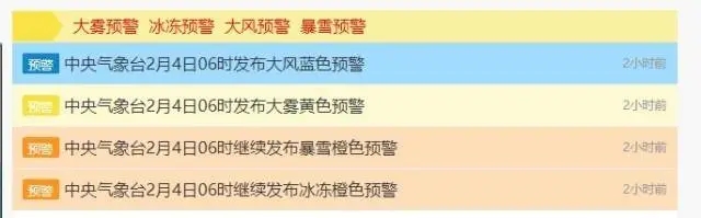 中央气象台连发四则气象灾害预警
暴雪橙色预警+冰冻橙色预警+大雾黄色预警+
资讯
中央气象台连发四则气象灾害预警
暴雪橙色预警+冰冻橙色预警+大雾黄色预警+
资讯